Nanoelectronics
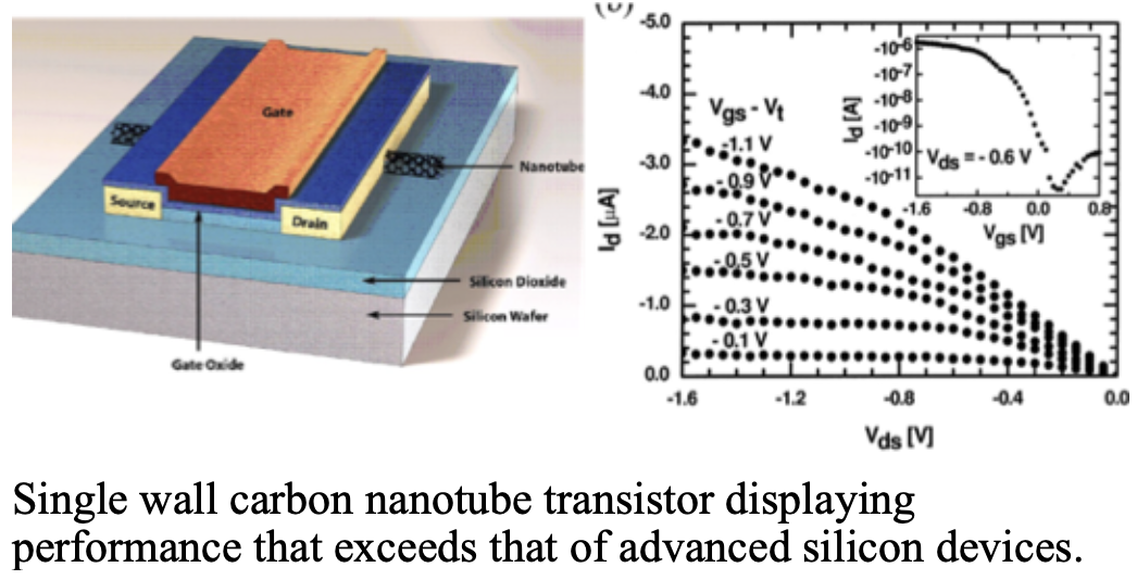
- Carbon nanotube electronics – The semiconductor industry has, for years, been seeking alternatives to traditional silicon scaling, which is the systematic reduction of transistor size that has fueled the incredible growth in computational speed and power, but which faces ultimate physical limits in the coming decade(s). New materials, such as semiconductor nanowires and carbon nanotubes, have outstanding electronic properties and have shown great promise for future applications, yet they face some significant challenges to implementation.
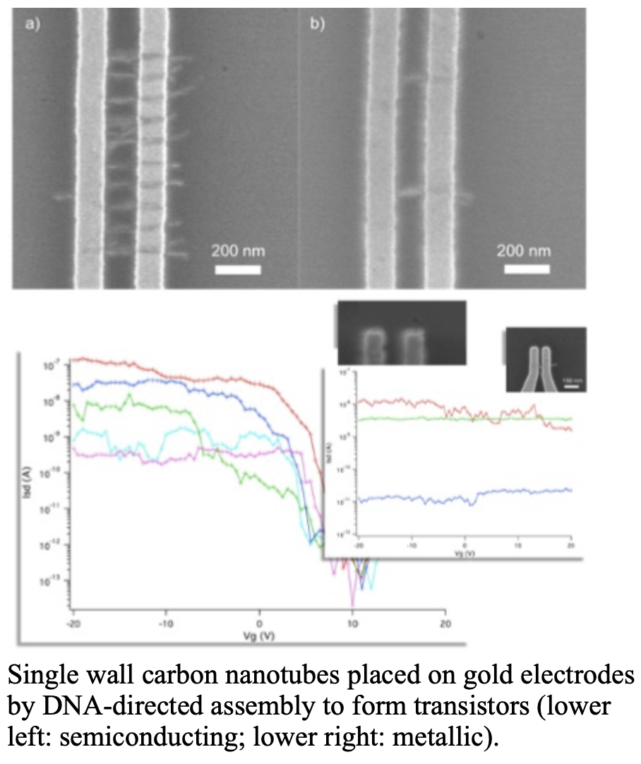
- Biological and Biologically Inspired Assembly of Functional Nanostructures – Self-assembly is playing continues to attract the attention of the semiconductor industry as a possible path to alleviating some of the demands of traditional lithographic patterning. A potential alternative, especially for non-silicon electronic devices, is the use of biological molecules to mediate the assembly of functional nanomaterials, such as carbon nanotubes, semiconducting nanowires, graphene sheets, or metallic nanoparticles for, e.g., plasmonic applications.As an example, we have been exploring new ways of forming carbon nanotube devices and circuits by organizing them on surfaces using a combination of nanolithgraphic patterning and DNA assembly.
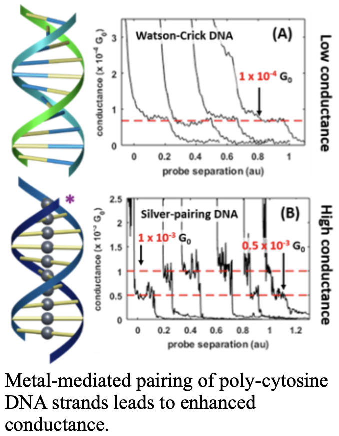
- Bioelectronics – Biomolecules, in general, have attracted interest as possible molecular switches primarily because of their potential for self-assembly and a vision of low-cost device fabrication, compared to conventional semiconductor electronics. Particular attention over the years has been given to DNA for (a) its one-dimensionality and (b) its programmability, in terms of sequencing and length. Thus far, whilst there have been reports of charge transport and switching in DNA, there has been clear demonstrations that DNA can be metalized to form a conducting wire. More recently, work out of the Wind lab at Columbia and other groups have shown that certain base pair mismatches can support the insertion of metal atoms and that concatenated strings of these display enhanced conductance. Further, these metal-mediated base pair sequences can be incorporated into self-assembling DNA nanostructures (e.g., DNA origami), raising the possibility of self-assembled DNA circuits.
Quantum Nanosystems – A hallmark of the nanoscale is the emergence of quantum mechanical phenomena. Innovative nanofabrication schemes can be brought to bear to create a wide variety of advanced quantum nanosystems with exquisite precision. Some examples include artificial graphene and nitrogen vacancy (NV) centers in diamond.
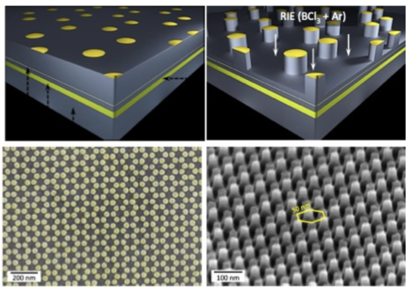
- Artificial graphene – Graphene, an atomically thin, two-dimensional allotrope of carbon, took the nanoscience community by storm, beginning in 2005. Its unusual electronic properties can be attributed in large part to the triangular symmetry of its hexagonal lattice. These properties can be simulated in a conventional semiconductor, GaAs (gallium arsenide) by imposing an hexagonal lattice upon a two-dimensional electron gas (2DEG) formed in a thin layer in the semiconductor. The ability to engineer the artificial graphene lattice parameters offers some fascinating possibilities for realizing new classes of exotic quantum phenomena.
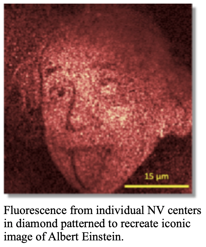
- NV centers in diamond – Nitrogen vacancy centers are a type of defect in diamond consisting of a nitrogen dopant adjacent to a missing carbon atom (vacancy) in the diamond crystal lattice. These defects form a sort of artificial atom that, when excited by a laser, can display long-lasting coherent spin states. Such states are of interest for possible future quantum information processing and communications applications. We are exploring new approaches for engineering and controlling NV centers using both advanced lithographic and biomolecular assembly techniques.
