Nanofabrication
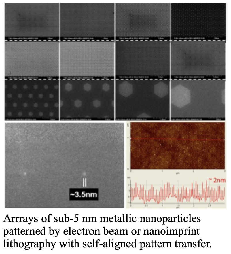
- Nanolithography and nanopatterning – Wind Nanoscience Advisors, Inc. has extensive experience in a wide range of lithography technologies, including optical, x-ray, electron beam and nanoimprint – particularly at the outer limits of the techniques’ resolution limits. In addition, a variety of innovative techniques, such as self-aligned patterning, sidewall and angled deposition, etc. can be used to achieve sub-resolution minimum features. Features as small as ~ 2 nm have been achieved using such approaches.
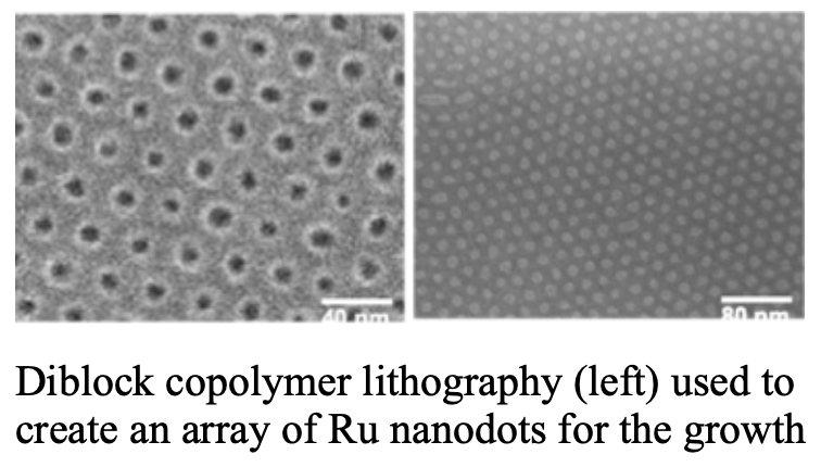
- Self-assembly and directed self-assembly – A variety of polymer systems (e.g., diblock copolymers) are available for creating repeating patterns with nanoscale dimensions over very large areas. These patterns typically lack long-range order, but under some circumstances, they may be combined with conventional lithography (optical, e-beam, nanoimprint) to form periodic structures over large areas or exclusively selected regions.

- Thin film processes – The term “nanotechnology” was first used in 1974 to describe the thin films that were less than 100 nm used in semiconductor devices. Such films are integral parts of nanofabrication, and different thin film combinations, combined with lithographic patterning (of any kind) can lead to innovative structures and functionality.
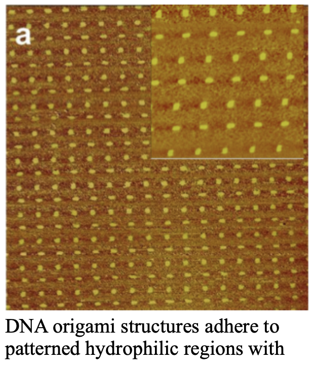
- Selective surface chemistry – Some applications, particularly (but not exclusively) in biology, require precise control over interactions between the background surface, patterned features, and samples or entities that are plated upon the surface. Control over chemical binding, through different combinations of passivation layers and/or adhesion layers, can be a crucial factor in achieving single-molecule control over interactions of interest.
